Constantly evolving

Our commitment to Research and Development
In the field of wireless communication in which the company operates, investing in Research and Development is a priority in order to be competitive in the ID market.
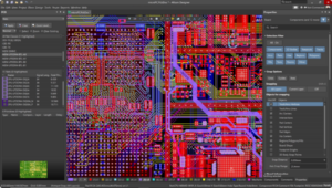
 TechSigno has over 15 years of in-depth experience in the field of schematics, layout, validation, testing and other aspects of microelectronic design. With an extensive circuit library, stack-up layout, modular test infrastructure, and other reusable hardware blocks, we can efficiently design complex and reliable embedded hardware.
The know-how gathered over the years allows TechSigno to offer the maximum flexibility in the creation of firmware and software through the most popular programming languages: C, C++, C#, Java and Python, used with experience to increase the hardware’s potential.
CPU and MCU Architectures:
- 8- and 16-bit microcontrollers (NXP, SiliconLabs, STMicroelectronics)
- Arm Cortex -A5, A7, -A8, -A9, -A15; Cortex-M0, -M4, -M7; Classic ARM7, ARM9, ARM11 (NXP/Freescale, Texas Instrument, Microchip/Atmel, STMicroelectronics)
- ColdFire® (NXP/Freescale)
- Power Architecture® (NXP/Freescale)
Circuits and Interfaces:
- DSP, FPGA, PLD, RTC
- Power: Power management; Reverse voltage protection; ESD and transient protection; Power Isolation; Power over Ethernet; Design for Automotive, Aircraft, Railway or Military standards compliance
- Memory and Storage: DDR4, NAND, NOR, SATA, SD/SDIO/MMC, SDRAM, SSD, SPI
- Connectivity: Bluetooth, CAN, Ethernet, PCle, SATA, USB, WiFi
- Serial ports: A/D, D/A, GPIO, I2C, SPI, UART and analog
- HMI: CSI, DVI, HDMI, LCD, LVDS, MIPI
- Multimedia: audio, video
- Embedded Vision: CMOS sensors, thermal cameras and other digital camera technology
Software Design:
- Bootloaders
- Device Drivers (Bluetooth, Camera, Display, GPS, WiFi)
- Firmware Embedded
- Hardware Abstraction Layer
- User-friendly graphical user interfaces
- Native Apps for a mobile device’s operating system
- Web Apps
Engineering:
- Design for Manufacturability and Design for Test optimization through close engineering and industrialization collaboration
- Common Data Exchange Engineering and Manufacturing: Bills of Material, CAD design data
Design Verification:
- Simulation
- Voltage, Current, Power, Timing, Signal Integrity and EMI Measurement
- Functional Test
- PCBA Microsection Analysis including PCB stack-up, solder mask and cross sectional metallographic examination
- HALT (Highly Accelerated Life Test) stress testing for revealing of product failure modes
- Radiated Emission, Conducted Emissions and Radiated Immunity Testing
- MTBF (Mean Time Between Failures) predictive performance and error probability calculations
- JTAG + Boundary Scan
- Signal Integrity (analysis of the impedance, stack-up and crosstalk)
- Production test: electrical, functional, boundary scan; modular test framework for rapid test adaptation
- Bed of nail, spring probe and fixture design
- Prototype housing
- Prototype mechanical parts
TechSigno is system-oriented with a strong verticalization on the market, which we obtained thanks to the knowledge acquired over time and the professionalism of the specialists of our team. The investment of resources to increase internal skills and know-how makes it possible for partners, operating in increasingly challenging sectors, to receive the necessary support throughout the entire implementation cycle of the devices.
Collaborations with Research Institutes and Institututions represent a large part of our corporate investments for Development.

TechSigno certified quality
TechSigno internal procedures provide for the complete control of the quality of materials, of the workforce, passing through aspects related to production such as qualifications, compliance, certifications and standards which include:
Origin declaration
REACH declaration
RoHS declaration


